Ch2: Common Op Amps Configurations
Op Amps Table of Contents
Unity Gain Buffer

To build a unity gain buffer, you simply connect the input to the non-inverting pin and feedback the output to the inverting pin. It’s a very simple circuit and gives you an amplifier circuit with a gain of 1. This might not seem like a very useful feature, but check out this video to learn more about this circuit:
This video describes the connections and purposes of a unity gain buffer and shows why an infinite open loop voltage gain leads to unity gain when you have negative feedback.
Unity Gain Amplifier Practice Problems
Question 1. (Click on arrow for answer)
Write the transfer function (input/output equation) for an operational amplifier with an open-loop voltage gain of 100,000, and the inverting input connected directly to its output terminal. In other words, write an equation describing the output voltage of this op-amp ([latex]V_{out}[/latex]) for any given input voltage at the noninverting input ([latex]V_{in(+)}[/latex]):

Then, once you have an equation written, solve for the over-all voltage gain ([latex]A_V = {V_{out} \over V_{in(+)}}[/latex]) of this amplifier circuit, and calculate the output voltage for a noninverting input voltage of +6 volts.
File Num: 00927
Answer
[latex]V_{out} = 100,000(V_{in(+)} – V_{out})[/latex](I’ve left it up to you to perform the algebraic simplification here!)[latex]A_V = {100,000 \over 100,001} = 0.99999[/latex]For an input voltage of +6 volts, the output voltage will be +5.99994 volts.
Notes
The significant point of this question is that students see the over-all voltage gain of the opamp radically attenuated from 100,000 to approximately 1. What is not so evident is just how stable this new voltage gain is, which is one of the purposes for employing negative feedback.
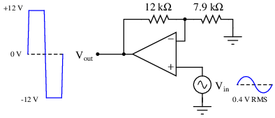
Question 2. (Click on arrow for answer)
How much effect will a change in the op-amp’s open-loop voltage gain have on the overall voltage gain of a negative-feedback circuit such as this?

If the open-loop gain of this operational amplifier were to change from 100,000 to 200,000, for example, how big of an effect would it have on the voltage gain as measured from the noninverting input to the output?
File Num: 02288
Answer
The different in overall voltage gain will be trivial.
Follow-up question: what advantage is there in building voltage amplifier circuits in this manner, applying negative feedback to a “core” amplifier with very high intrinsic gain?
Notes
Work with your students to calculate a few example scenarios, with the old open-loop gain versus the new open-loop gain. Have the students validate their conclusions with numbers!
Negative feedback is an extremely useful engineering principle, and one that allows us to build very precise amplifiers using imprecise components. Credit for this idea goes to Harold Black, an electrical engineer, in 1920’s. Mr. Black was looking for a way to improve the linearity and stability of amplifiers in telephone systems, and (as legend has it) the idea came to him in a flash of insight as he was commuting on a ferry boat.
An interesting historical side-note is that Black’s 1928 patent application was initially rejected on the grounds that he was trying to submit a perpetual motion device! The concept of negative feedback in an amplifier circuit was so contrary to established engineering thought at the time, that Black experienced significant resistance to the idea within the engineering community. The United States patent office, on the other hand, was inundated with fraudulent “perpetual motion” claims, and so dismissed Black’s invention at first sight.
Question 3. (Click on arrow for answer)
Complete the table of voltages for this opamp “voltage follower” circuit:
 $$\vbox{\offinterlineskip
\halign{\strut
\vrule \quad\hfil # \ \hfil &
\vrule \quad\hfil # \ \hfil \vrule \cr
\noalign{\hrule}[latex]V_{in}[/latex] & [latex]V_{out}[/latex] \cr\noalign{\hrule}
0 volts & 0 volts \cr
\noalign{\hrule}+5 volts & \cr\noalign{\hrule}+10 volts & \cr\noalign{\hrule}+15 volts & \cr\noalign{\hrule}+20 volts & \cr\noalign{\hrule}-5 volts & \cr\noalign{\hrule}-10 volts & \cr\noalign{\hrule}-15 volts & \cr\noalign{\hrule}-20 volts & \cr\noalign{\hrule}
} % End of \halign
}$$ % End of \vboxFile Num: 02289
Answer
$$\vbox{\offinterlineskip \halign{\strut \vrule \quad\hfil # \ \hfil & \vrule \quad\hfil # \ \hfil \vrule \cr \noalign{\hrule}[latex]V_{in}[/latex] & [latex]V_{out}[/latex] \cr\noalign{\hrule}0 volts & 0 volts \cr
\noalign{\hrule}+5 volts & +5 volts \cr\noalign{\hrule}+10 volts & +10 volts \cr\noalign{\hrule}+15 volts & +15 volts \cr\noalign{\hrule}+20 volts & +15 volts \cr\noalign{\hrule}-5 volts & -5 volts \cr\noalign{\hrule}-10 volts & -10 volts \cr\noalign{\hrule}-15 volts & -15 volts \cr\noalign{\hrule}-20 volts & -15 volts \cr\noalign{\hrule} } % End of \halign }$$ % End of \vboxFollow-up question: the output voltage values given in this table are ideal. A real opamp would probably not be able to achieve even what is shown here, due to idiosyncrasies of these amplifier circuits. Explain what would probably be different in a real opamp circuit from what is shown here.
Notes
A common mistake I see students new to opamps make is assuming that the output voltage will magically attain whatever value the gain equation predicts, with no regard for power supply rail voltage limits.
Another good follow-up question to ask your students is this: “How much voltage is there between the two input terminals in each of the situations described in the table?” They will find that the “golden rule” of closed-loop opamp circuits can be violated!
If students have difficulty answering the follow-up question, drop these two hints: (1) Rail-to-rail output swing and (2) Latch-up.
Question 4. (Click on arrow for answer)
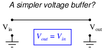
This operational amplifier circuit is often referred to as a voltage buffer, because it has unity gain (0 dB) and therefore simply reproduces, or “buffers,” the input voltage:

What possible use is a circuit such as this, which offers no voltage gain or any other form of signal modification? Wouldn’t a straight piece of wire do the same thing? Explain your answers.

File Num: 03801
Answer
While this circuit offers no voltage gain, it does offer current gain and impedance transformation. Much like the common-collector (or common-drain) single transistor amplifier circuits which also had voltage gains of (near) unity, opamp buffer circuits are useful whenever one must drive a relatively “heavy” (low impedance) load with a signal coming from a “weak” (high impedance) source.
Notes
I have found that some students have difficulty with the terms “heavy” and “light” in reference to load characteristics. That a “heavy” load would have very few ohms of impedance, and a “light” load would have many ohms of impedance seems counter-intuitive to some. It all makes sense, though, once students realize the terms “heavy” and “light” refer to the amount of current drawn by the respective loads.
Ask your students to explain why the straight piece of wire fails to “buffer” the voltage signal in the same way the the opamp follower circuit does.
Question 5. (Click on arrow for answer)
For all practical purposes, how much voltage exists between the inverting and noninverting input terminals of an op-amp in a functioning negative-feedback circuit?
File Num: 00930
Answer
Zero volts
Notes
Ask your students to explain why there will be (practically) no voltage between the input terminals of an operational amplifier when it is used in a negative feedback circuit.
Question 6. (Click on arrow for answer)
Just as certain assumptions are often made for bipolar transistors in order to simplify their analysis in circuits (an ideal BJT has negligible base current, [latex]I_C = I_E[/latex], constant [latex]\beta[/latex], etc.), we often make assumptions about operational amplifiers so we may more easily analyze their behavior in closed-loop circuits. Identify some of these ideal opamp assumptions as they relate to the following parameters:
- Magnitude of input terminal currents:
- Input impedance:
- Output impedance:
- Input voltage range:
- Output voltage range:
- Differential voltage (between input terminals) with negative feedback:
File Num: 02749
Answer
- Magnitude of input terminal currents: infinitesimal
- Input impedance: infinite
- Output impedance: infinitesimal
- Input voltage range: never exceeding +V/-V
- Output voltage range: never exceeding +V/-V
- Differential voltage (between input terminals) with negative feedback: infinitesimal
Notes
Just in case your students are unfamiliar with the words infinite and infinitesimal, tell them they simply mean “bigger than big” and “smaller than small”, respectively.
Question 7. (Click on arrow for answer)
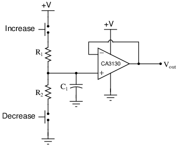
The purpose of this circuit is to provide a pushbutton-adjustable voltage. Pressing one button causes the output voltage to increase, while pressing the other button causes the output voltage to decrease. When neither button is pressed, the voltage remains stable:

After working just fine for quite a long while, the circuit suddenly fails: now it only outputs zero volts DC all the time.
An experienced technician first checks the power supply voltage to see if it is within normal limits, and it is. Then, the technician checks the voltage across the capacitor. Explain why this is a good test point to check, and what the results of that check would tell the technician about the nature of the fault.
File Num: 03773
Answer
Checking for voltage across the capacitor will tell the technician what voltage the op-amp follower is being “told” to reproduce at the output.
Challenge question: why do you suppose I specify a CA3130 operational amplifier for this particular circuit? What is special about this opamp that qualifies it for the task?
Notes
Knowing where to check for critical signals in a circuit is an important skill, because it usually means the difference between efficiently locating a fault and wasting time. Ask your students to explain in detail the rationale behind checking for voltage across the capacitor, and (again, in detail) what certain voltage measurements at that point would prove about the nature of the fault.
Inverting Amplifier Circuit

An inverting amplifier is one where the output is inverted, or phase shifted by 180o compared to the input. This is another simple circuit, but a little more complicated than the unity gain buffer. See this video to learn more:
This video shows why the amplifier is called an “inverting” one and shows how to figure out the voltage gain based on the input and feedback resistor. It also includes an LTSpice simulation to demonstrate how the amplifier works.
Non-Inverting Amplifier Practice Problems
Question 1. (Click on arrow for answer)
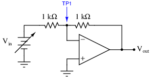
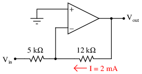
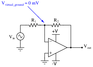
Trace the directions for all currents in this circuit, and calculate the values for voltage at the output ([latex]V_{out}[/latex]) and at test point 1 ([latex]V_{TP1}[/latex]) for several values of input voltage ([latex]V_{in}[/latex]):

Vin Vtp1 Vout 0.0V 0.4V 1.2V 3.4V 7.1V 10.8V
Then, from the table of calculated values, determine the voltage gain ([latex]A_V[/latex]) for this amplifier circuit.
File Num: 02467
Answer

| Vin | Vtp1 | Vout |
|---|---|---|
| 0.0V | 0.0V | 0.0V |
| 0.4V | 0.0V | -0.4V |
| 1.2V | 0.0V | -1.2V |
| 3.4V | 0.0V | -3.4V |
| 7.1V | 0.0V | -7.1V |
| 10.8V | 0.0V | -10.8V |
Follow-up question: the point marked “TP1” in this circuit is often referred to as a virtual ground. Explain why this is, based on the voltage figures shown in the above table.
Notes
Some texts describe the voltage gain of an inverting voltage amplifier as being a negative quantity. I tend not to look at things that way, treating all gains as positive quantities and relying on my knowledge of circuit behavior to tell whether the signal is inverted or not. In my teaching experience, I have found that students have a tendency to blindly follow equations rather than think about what it is they are calculating, and that strict adherence to the mathematical signs of gain values only encourages this undesirable behavior (“If the sign of the gain tells me whether the circuit is inverting or not, I can just multiply input voltage by gain and the answer will always be right!”).
This strategy is analogous to problem-solving in electromagnetics, where a common approach is to use math to solve for the absolute values of quantities (potential, induced voltage, magnetic flux), and then to use knowledge of physical principles (Lenz’ Law, right-hand rule) to solve for polarities and directions. The alternative — to try to maintain proper sign convention throughout all calculations — not only complicates the math but it also encourages students to over-focus on calculations and neglect fundamental principles.
Question 2. (Click on arrow for answer)
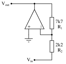
Calculate the overall voltage gain of this amplifier circuit ([latex]A_V[/latex]), both as a ratio and as a figure in units of decibels (dB). Also, write a general equation for calculating the voltage gain of such an amplifier, given the resistor values of [latex]R_1[/latex] and [latex]R_2[/latex]:

File Num: 02458
Answer
[latex]A_V = 1 = 0[/latex] dB[latex]A_V = {R_1 \over R_2} \hbox{ (expressed as a ratio, not dB)}[/latex]Follow-up question \#1: sometimes the voltage gain equation for an amplifier of this type is given in the following form:
[latex]A_V = -{R_1 \over R_2}[/latex]What is the significance of the negative sign in this equation? Is it really necessary, or does it communicate an important concept?
Follow-up question \#2: manipulate the gain equation for this amplifier circuit to solve for the value of resistor [latex]R_1[/latex].
Notes
Whether inverting amplifier gains are expressed as negative or positive quantities seems to be a matter of taste, from surveying introductory textbooks on the subject. I prefer to stick with absolute (positive) gain values and consider signal inversion separately.
Question 3. (Click on arrow for answer)
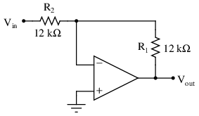
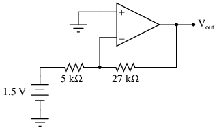
Calculate all voltage drops and currents in this circuit, complete with arrows for current direction and polarity markings for voltage polarity. Then, calculate the overall voltage gain of this amplifier circuit ([latex]A_V[/latex]), both as a ratio and as a figure in units of decibels (dB):

File Num: 02468
Answer
 [latex]A_V[/latex] = 0.468 = -6.594 dB
Notes
Operational amplifier circuits provide a great opportunity to review basic concepts of DC circuits: voltage drops, polarity, current directions, Ohm’s Law, Kirchhoff’s Voltage Law, Kirchhoff’s Current Law, etc. This circuit is no exception. Emphasize the fact that a great many opamp circuits may be comprehensively analyzed merely with knowledge of these fundamental principles and the characteristics of an ideal opamp (zero input current, infinite open-loop gain, unlimited output voltage swing, zero voltage between input terminals when negative feedback is in effect).
Some students may arrive at the wrong gain figure because they blindly followed a formula with [latex]R_1[/latex] and [latex]R_2[/latex] shown as variables, plugging in this circuit’s values for [latex]R_1[/latex] and [latex]R_2[/latex] without considering which resistor is which (is [latex]R_1[/latex] the feedback resistor or is [latex]R_2[/latex]?). This is by design, as I want students to learn to think about what they are doing rather than thoughtlessly follow instructions.
Question 4. (Click on arrow for answer)
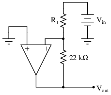
Determine both the input and output voltage in this circuit:

File Num: 02732
Answer
[latex]V_{in}[/latex] = -10 V. [latex]V_{out}[/latex] = 24 VFollow-up question: how do we know that the input voltage in this circuit is negative and the output voltage is positive?
Notes
Ask your students how they solved this problem, sharing techniques and strategies to help other students know where to begin and where to proceed from there.
Question 5. (Click on arrow for answer)
The equation for voltage gain ([latex]A_V[/latex]) in a typical inverting, single-ended opamp circuit is as follows:
[latex]A_V = {R_{1} \over R_{2}}[/latex]
Where,
[latex]R_1[/latex] is the feedback resistor (connecting the output to the inverting input)[latex]R_2[/latex] is the other resistor (connecting the inverting input to voltage signal input terminal)
Suppose we wished to change the voltage gain in the following circuit from 3.5 to 4.9, but only had the freedom to alter the resistance of [latex]R_{2}[/latex]:

Algebraically manipulate the gain equation to solve for [latex]R_2[/latex], then determine the necessary value of [latex]R_2[/latex] in this circuit to give it a voltage gain of 4.9.
File Num: 02708
Answer
[latex]R_2 = {R_1 \over A_V}[/latex]For the circuit shown, [latex]R_2[/latex] would have to be set equal to 1.571 k[latex]\Omega[/latex].
Notes
Nothing more than a little algebra to obtain the answers for this question!
Question 6. (Click on arrow for answer)
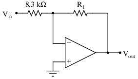
Calculate the necessary resistor value ([latex]R_1[/latex]) in this circuit to give it a voltage gain of 15:

File Num: 02729
Answer
[latex]R_1[/latex] = 1.467 k[latex]\Omega[/latex]Notes
Ask your students how they solved this problem, especially since it is fairly safe to say that they didn’t find the equation directly solving for [latex]R_1[/latex] in any book. Algebraic manipulation is necessary to take the standard voltage gain equation and put it into a form suitable for use answering this question.
Question 7. (Click on arrow for answer)
Calculate the necessary resistor value ([latex]R_1[/latex]) in this circuit to give it a voltage gain of 7.5:

File Num: 02730
Answer
[latex]R_1[/latex] = 62.25 k[latex]\Omega[/latex]Notes
Ask your students how they solved this problem, especially since it is fairly safe to say that they didn’t find the equation directly solving for [latex]R_1[/latex] in any book. Algebraic manipulation is necessary to take the standard voltage gain equation and put it into a form suitable for use answering this question.
Question 8. (Click on arrow for answer)
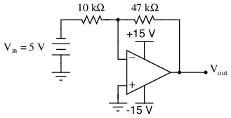
Calculate the output voltage of this op-amp circuit (using negative feedback):

Also, calculate the DC voltage gain of this circuit.
File Num: 00932
Answer
[latex]V_{out} =[/latex] -8.1 volts[latex]A_V =[/latex] 5.4
Follow-up question: the midpoint of the voltage divider (connecting to the inverting input of the op-amp) is often called a virtual ground in a circuit like this. Explain why.
Notes
It is important that students learn to analyze the op-amp circuit in terms of voltage drops and currents for each resistor, rather than just calculate the output using a gain formula. Detailed, Ohm’s Law analysis of op-amp circuits is essential for analyzing more complex circuitry.
The “virtual ground” question is an important one for the sake of rapid analysis. Once students understand how and why there is such a thing as a “virtual ground” in an op-amp circuit like this, their analysis of op-amp circuits will be much more efficient.
Question 9. (Click on arrow for answer)
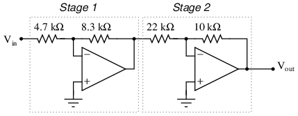
Calculate the voltage gain for each stage of this amplifier circuit (both as a ratio and in units of decibels), then calculate the overall voltage gain:

File Num: 02470
Answer
- Stage 1: [latex]A_V[/latex] = 1.5 = 3.522 dB
- Stage 2: [latex]A_V[/latex] = 1.545 = 3.781 dB
- Total: [latex]A_V[/latex] = 2.318 = 7.303 dB
Notes
Not only does this question review calculation of voltage gain for inverting amplifier circuits, but it also reviews decibel calculations (for both single and multi-stage amplifiers). Discuss how the decibel figures for each stage add to equal the total decibel gain, whereas the ratios multiply.
Question 10. (Click on arrow for answer)
Calculate the voltage gain for each stage of this amplifier circuit (both as a ratio and in units of decibels), then calculate the overall voltage gain:

File Num: 02471
Answer
- Stage 1: [latex]A_V[/latex] = 1.766 = 4.940 dB
- Stage 2: [latex]A_V[/latex] = 0.455 = -6.848 dB
- Total: [latex]A_V[/latex] = 0.803 = -1.909 dB
Notes
Not only does this question review calculation of voltage gain for inverting amplifier circuits, but it also reviews decibel calculations (for both single and multi-stage amplifiers). Discuss how the decibel figures for each stage add to equal the total decibel gain, whereas the ratios multiply.
Question 11. (Click on arrow for answer)
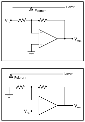
Operational amplifier circuits employing negative feedback are sometimes referred to as “electronic levers,” because their voltage gains may be understood through the mechanical analogy of a lever. Explain this analogy in your own words, identifying how the lengths and fulcrum location of a lever relate to the component values of an op-amp circuit:

File Num: 00933
Answer
The analogy of a lever works well to explain how the output voltage of an op-amp circuit relates to the input voltage, in terms of both magnitude and polarity. Resistor values correspond to moment arm lengths, while direction of lever motion (up versus down) corresponds to polarity. The position of the fulcrum represents the location of ground potential in the feedback network.
Notes
I found this analogy in one of the best books I’ve ever read on op-amp circuits: John I. Smith’s Modern Operational Circuit Design. Unfortunately, this book is out of print, but if you can possibly obtain a copy for your library, I highly recommend it!
Question 12. (Click on arrow for answer)
Compare and contrast inverting versus noninverting amplifier circuits constructed using operational amplifiers:

How do these two general forms of opamp circuit compare, especially in regard to input impedance and the range of voltage gain adjustment?
File Num: 02469
Answer
The noninverting configuration exhibits a far greater input impedance than the inverting amplifier, but has a more limited range of voltage gain: always greater than or equal to unity.
Notes
Just a simple comparison between amplifier configurations, nothing more. Ask your students to elaborate on the inverting amplifier’s range of gain adjustment: how does it differ from the noninverting configuration?
Question 13. (Click on arrow for answer)
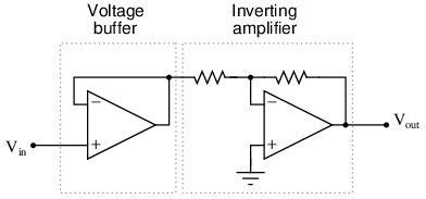
What possible benefit is there to adding a voltage buffer to the front end of an inverting amplifier, as shown in the following schematic?

File Num: 02472
Answer
The voltage buffer raises the amplifier’s input impedance without altering voltage gain.
Notes
Discuss with your students how this is very common: using a voltage buffer as an impedance transformation (or isolation) device so that a weak (high-impedance) source is able to drive an amplifier.
Question 14. (Click on arrow for answer)
The junction between the two resistors and the inverting input of the operational amplifier is often referred to as a virtual ground, the voltage between it and ground being (almost) zero over a wide range of circuit conditions:

If the operational amplifier is driven into saturation, though, the “virtual ground” will no longer be at ground potential. Explain why this is, and what condition(s) may cause this to happen.
Hint: analyze all currents and voltage drops in the following circuit, assuming an opamp with the ability to swing its output voltage rail-to-rail.

File Num: 02473
Answer
Any input signal causing the operational amplifier to try to output a voltage beyond either of its supply rails will cause the “virtual ground” node to deviate substantially from ground potential.
Notes
Before students can answer this question, they must understand what saturation means with regard to an operational amplifier. This is where the “hint” scenario comes into play. Students failing to grasp this concept will calculate the voltage drops and currents in the “hint” circuit according to standard procedures and assumptions, and arrive at an output voltage well in excess of +15 volts. Resolving this paradox will lead to insight, and hopefully to a more realistic set of calculations.
Question 15. (Click on arrow for answer)
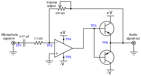
There is something wrong with this amplifier circuit. Despite an audio signal of normal amplitude detected at test point 1 (TP1), there is no output measured at the “Audio signal out” jack:

Next, you decide to check for the presence of a good signal at test point 3 (TP3). There, you find 0 volts AC and DC no matter where the volume control is set.
From this information, formulate a plan for troubleshooting this circuit, answering the following questions:
- What type of signal would you expect to measure at TP3?
- What would be your next step in troubleshooting this circuit?
- Are there any elements of this circuit you know to be working properly?
- What do you suppose would be the most likely failure, assuming this circuit once worked just fine and suddenly stopped working all on it’s own?
File Num: 02474
Answer
The correct voltage signal at TP3 should be an audio waveform with significant crossover distortion (specifically, a vertical “jump” at each point where the waveform crosses zero volts, about 1.4 volts peak to peak). I’ll let you figure out answers to the other questions on your own, or with classmates.
Notes
I have found that troubleshooting scenarios are always good for stimulating class discussions, with students posing strategies for isolating the fault(s) and correcting one another on logical errors. There is not enough information given in this question to ensure a single, correct answer. Discuss this with your students, helping them to use their knowledge of circuit theory and opamps to formulate good diagnostic strategies.
Non-Inverting Amplifier Circuit
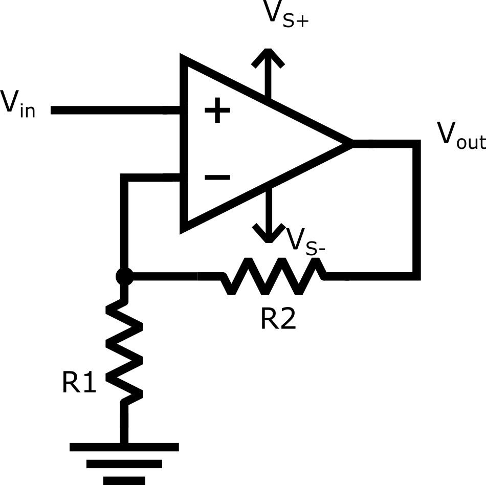
A non-inverting amplifier does not invert that output (as you probably suspected). It does use negative feedback like the inverting amplifier to give a gain that is controllable by the external resistors. Check out this video for the details.
This video shows the configuration of a non-inverting op amp circuit and shows how to derive the equation for the gain of the amplifier. It even includes some simulations to show the op amp in action
Non-Inverting Amplifier Practice Problems
Question 1. (Click on arrow for answer)
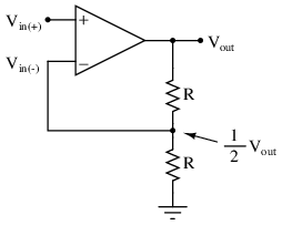
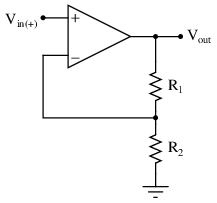
Write the transfer function (input/output equation) for an operational amplifier with an open-loop voltage gain of 100,000, and the inverting input connected to a voltage divider on its output terminal (so the inverting input receives exactly one-half the output voltage). In other words, write an equation describing the output voltage of this op-amp ([latex]V_{out}[/latex]) for any given input voltage at the noninverting input ([latex]V_{in(+)}[/latex]):

Then, once you have an equation written, solve for the output voltage if the noninverting input voltage is -2.4 volts.
File Num: 00928
Answer
[latex]V_{out} = 100,000(V_{in(+)} – {1 \over 2}V_{out})[/latex](I’ve left it up to you to perform the algebraic simplification here!)\vskip 20pt
For an input voltage of -2.4 volts, the output voltage will be -4.7999 volts.
Follow-up question: what do you notice about the output voltage in this circuit? What value is it very close to being, in relation to the input voltage? Does this pattern hold true for other input voltages as well?
Notes
Your students should see a definite pattern here as they calculate the output voltage for several different input voltage levels. Discuss this phenomenon with your students, asking them to explain it as best they can.
Question 2. (Click on arrow for answer)
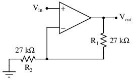
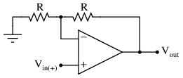
Calculate the overall voltage gain of this amplifier circuit ([latex]A_V[/latex]), both as a ratio and as a figure in units of decibels (dB). Also, write a general equation for calculating the voltage gain of such an amplifier, given the resistor values of [latex]R_1[/latex] and [latex]R_2[/latex]:

File Num: 02457
Answer
[latex]A_V = 2 = 6.02[/latex] dB[latex]A_V = {R_1 \over R_2} + 1 \hbox{ (expressed as a ratio, not dB)}[/latex]Follow-up question: explain how you could modify this particular circuit to have a voltage gain (ratio) of 3 instead of 2.
Notes
Nothing special here — just some practice with voltage gain calculations.
Question 3. (Click on arrow for answer)
What would have to be altered in this circuit to increase its overall voltage gain?

File Num: 00931
Answer
The voltage divider would have to altered so as to send a smaller proportion of the output voltage to the inverting input.
Notes
Ask your students to explain how they would modify the voltage divider in this circuit to achieve the goal of a smaller voltage division ratio. This should be trivial, but it is always good to review basic principles of electricity even when “deep” into a more advanced topic.
Question 4. (Click on arrow for answer)
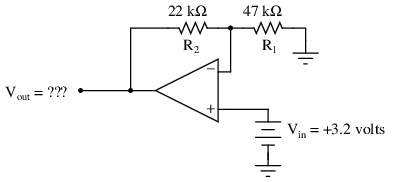
Calculate all voltage drops and currents in this circuit, complete with arrows for current direction and polarity markings for voltage polarity. Then, calculate the overall voltage gain of this amplifier circuit ([latex]A_V[/latex]), both as a ratio and as a figure in units of decibels (dB):

File Num: 02459
Answer
 [latex]A_V[/latex] = 1.468 = 3.335 dB
Notes
Operational amplifier circuits provide a great opportunity to review basic concepts of DC circuits: voltage drops, polarity, current directions, Ohm’s Law, Kirchhoff’s Voltage Law, Kirchhoff’s Current Law, etc. This circuit is no exception. Emphasize the fact that a great many opamp circuits may be comprehensively analyzed merely with knowledge of these fundamental principles and the characteristics of an ideal opamp (zero input current, infinite open-loop gain, unlimited output voltage swing, zero voltage between input terminals when negative feedback is in effect).
Some students may arrive at the wrong gain figure because they blindly followed a formula with [latex]R_1[/latex] and [latex]R_2[/latex] shown as variables, plugging in this circuit’s values for [latex]R_1[/latex] and [latex]R_2[/latex] without considering which resistor is which (is [latex]R_1[/latex] the feedback resistor or is [latex]R_2[/latex]?). This is by design, as I want students to learn to think about what they are doing rather than thoughtlessly follow instructions.
Question 5. (Click on arrow for answer)
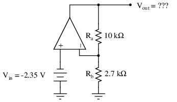
Calculate all voltage drops and currents in this circuit, complete with arrows for current direction and polarity markings for voltage polarity. Then, calculate the overall voltage gain of this amplifier circuit ([latex]A_V[/latex]), both as a ratio and as a figure in units of decibels (dB):

File Num: 02460
Answer
 [latex]A_V[/latex] = 4.704 = 13.449 dB
Follow-up question: how much input impedance does the -2.35 volt source “see” as it drives this amplifier circuit?
Notes
Operational amplifier circuits provide a great opportunity to review basic concepts of DC circuits: voltage drops, polarity, current directions, Ohm’s Law, Kirchhoff’s Voltage Law, Kirchhoff’s Current Law, etc. This circuit is no exception. Emphasize the fact that a great many opamp circuits may be comprehensively analyzed merely with knowledge of these fundamental principles and the characteristics of an ideal opamp (zero input current, infinite open-loop gain, unlimited output voltage swing, zero voltage between input terminals when negative feedback is in effect).
The follow-up question is important because it showcases one of the great advantages of using noninverting opamp amplifier circuits as voltage signal amplifiers: extremely high input impedance. This would be a good opportunity to review typical input impedance values for operational amplifiers, by showing datasheets for some typical opamps and for some non-typical (i.e. MOSFET input) opamps.
Question 6. (Click on arrow for answer)
[latex]\int f(x) dx[/latex] Calculus alert!
You are part of a team building a rocket to carry research instruments into the high atmosphere. One of the variables needed by the on-board flight-control computer is velocity, so it can throttle engine power and achieve maximum fuel efficiency. The problem is, none of the electronic sensors on board the rocket has the ability to directly measure velocity. What is available is an altimeter, which infers the rocket’s altitude (it position away from ground) by measuring ambient air pressure; and also an accelerometer, which infers acceleration (rate-of-change of velocity) by measuring the inertial force exerted by a small mass.
The lack of a “speedometer” for the rocket may have been an engineering design oversight, but it is still your responsibility as a development technician to figure out a workable solution to the dilemma. How do you propose we obtain the electronic velocity measurement the rocket’s flight-control computer needs?
File Num: 02702
Answer
One possible solution is to use an electronic integrator circuit to derive a velocity measurement from the accelerometer’s signal. However, this is not the only possible solution!
Notes
This question simply puts students’ comprehension of basic calculus concepts (and their implementation in electronic circuitry) to a practical test.
Question 7. (Click on arrow for answer)
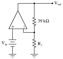
Calculate the necessary resistor value ([latex]R_1[/latex]) in this circuit to give it a voltage gain of 30:

File Num: 02725
Answer
[latex]R_1[/latex] = 1.345 k[latex]\Omega[/latex]Notes
Ask your students how they solved this problem, especially since it is fairly safe to say that they didn’t find the equation directly solving for [latex]R_1[/latex] in any book. Algebraic manipulation is necessary to take the standard voltage gain equation and put it into a form suitable for use answering this question.
Question 8. (Click on arrow for answer)
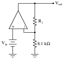
Calculate the necessary resistor value ([latex]R_1[/latex]) in this circuit to give it a voltage gain of 10.5:

File Num: 02724
Answer
[latex]R_1[/latex] = 76.95 k[latex]\Omega[/latex]Notes
Ask your students how they solved this problem, especially since it is fairly safe to say that they didn’t find the equation directly solving for [latex]R_1[/latex] in any book. Algebraic manipulation is necessary to take the standard voltage gain equation and put it into a form suitable for use answering this question.
Question 9. (Click on arrow for answer)
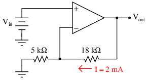
Determine both the input and output voltage in this circuit:

File Num: 02726
Answer
[latex]V_{in}[/latex] = 10 V. [latex]V_{out}[/latex] = 46 VNotes
Ask your students how they solved this problem, sharing techniques and strategies to help other students know where to begin and where to proceed from there.
Question 10. (Click on arrow for answer)
Calculate the voltage gain for each stage of this amplifier circuit (both as a ratio and in units of decibels), then calculate the overall voltage gain:

File Num: 02727
Answer
- [latex]A_V[/latex] = 4.3 = 12.669 dB
- [latex]A_V[/latex] = 6.745 = 16.579 dB
- [latex]A_V[/latex] = 29.002 = 29.249 dB
Notes
Not only does this question review calculation of voltage gain for inverting amplifier circuits, but it also reviews decibel calculations (for both single and multi-stage amplifiers). Discuss how the decibel figures for each stage add to equal the total decibel gain, whereas the ratios multiply.
Question 11. (Click on arrow for answer)
How much effect will a change in the op-amp’s open-loop voltage gain have on the overall voltage gain of a negative-feedback circuit such as this?

If the open-loop gain of this operational amplifier were to change from 100,000 to 200,000, for example, how big of an effect would it have on the voltage gain as measured from the noninverting input to the output?
File Num: 00929
Answer
The different in overall voltage gain will be trivial.
Follow-up question: what advantage is there in building voltage amplifier circuits in this manner, applying negative feedback to a “core” amplifier with very high intrinsic gain?
Notes
Work with your students to calculate a few example scenarios, with the old open-loop gain versus the new open-loop gain. Have the students validate their conclusions with numbers!
Negative feedback is an extremely useful engineering principle, and one that allows us to build very precise amplifiers using imprecise components. Credit for this idea goes to Harold Black, an electrical engineer, in 1920’s. Mr. Black was looking for a way to improve the linearity and stability of amplifiers in telephone systems, and (as legend has it) the idea came to him in a flash of insight as he was commuting on a ferry boat.
An interesting historical side-note is that Black’s 1928 patent application was initially rejected on the grounds that he was trying to submit a perpetual motion device! The concept of negative feedback in an amplifier circuit was so contrary to established engineering thought at the time, that Black experienced significant resistance to the idea within the engineering community. The United States patent office, on the other hand, was inundated with fraudulent “perpetual motion” claims, and so dismissed Black’s invention at first sight.
Question 12. (Click on arrow for answer)
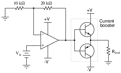
A simple “follower” circuit that boosts the current-output ability of this noninverting amplifier circuit is a set of bipolar junction transistors, connected together in a “push-pull” fashion like this:

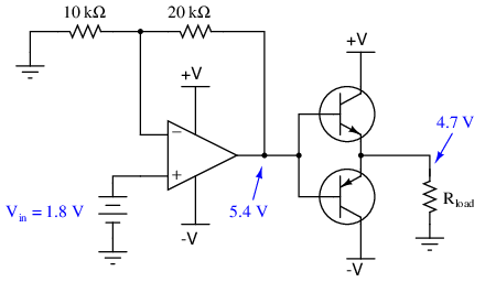
However, if connected exactly as shown, there will be a significant voltage error introduced to the opamp’s output. No longer will the final output voltage (measured across the load) be an exact 3:1 multiple of the input voltage, due to the 0.7 volts dropped by the transistor in active mode:

There is a very simple way to completely eliminate this error, without adding any additional components. Modify the circuit accordingly.
File Num: 00935
Answer

If you understand why this circuit works, pat yourself on the back: you truly understand the self-correcting nature of negative feedback. If not, you have a bit more studying to do!
Notes
The answer is not meant to be discouraging for those students of yours who do not understand how the solution works. It is simply a “litmus test” of whether or not your students really comprehend the concept of negative feedback. Although the change made in the circuit is simple, the principle is a bit of a conceptual leap for some people.
It might help your students understand if you label the new wire with the word sense, to indicate its purpose of providing feedback from the very output of the circuit, back to the opamp so it can sense how much voltage the load is receiving.
Question 13. (Click on arrow for answer)
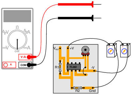
Suppose a technician is checking the operation of the following electronic circuit:

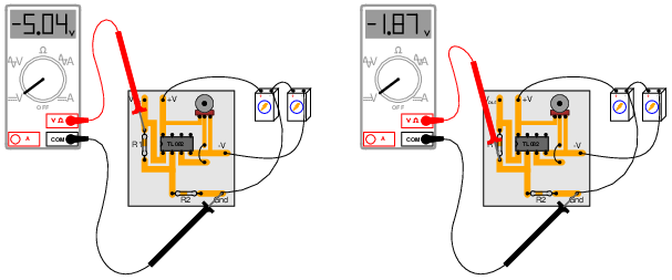
She decides to measure the voltage on either side of resistor R1 with reference to ground, and obtains these readings:

On the top side of R1, the voltage with reference to ground is -5.04 volts. On the bottom side of R1, the voltage with reference to ground is -1.87 volts. The color code of resistor R1 is Yellow, Violet, Orange, Gold. From this information, determine the following:
- Voltage across R1 (between top to bottom):
- Polarity (+ and -) of voltage across R1:
- Current (magnitude) through R1:
- Direction of current through R1:
Additionally, explain how this technician would make each one of these determinations. What rules or laws of electric circuits would she apply?
File Num: 02733
Answer
- Voltage across R1 (between top to bottom): 3.17 volts
- Polarity (+ and -) of voltage across R1: (-) on top, (+) on bottom
- Current (magnitude) through R1: 67.45 [latex]\mu[/latex]A
- Direction of current through R1: upward, following conventional flow
Follow-up question: calculate the range of possible currents, given the specified tolerance of resistor R1 (67.45 [latex]\mu[/latex]A assumes 0\% error).
Challenge question: if you recognize the type of circuit this is (by the part number of the IC “chip”: TL082), identify the voltage between pin 3 and ground.
Notes
This is a good example of how Kirchhoff’s Voltage Law is more than just an abstract tool for mathematical analysis — it is also a powerful technique for practical circuit diagnosis. Students must apply KVL to determine the voltage drop across R1, and then use Ohm’s Law to calculate its current.
If students experience difficulty visualizing how KVL plays a part in the solution of this problem, show them this illustration:

By the way, the answer to the challenge question may only be realized if students recognize this circuit as a noninverting opamp voltage amplifier. The voltage at pin 3 (noninverting input) will be the same as the voltage at pin 2 (inverting input): -1.87 volts.
Question 14. (Click on arrow for answer)
There is something wrong with this amplifier circuit. Note the relative amplitudes of the input and output signals as measured by an oscilloscope:

This circuit used to function perfectly, but then began to malfunction in this manner: producing a “clipped” output waveform of excessive amplitude. Determine the approximate amplitude that the output voltage waveform should be for the component values given in this circuit, and then identify possible causes of the problem and also elements of the circuit that you know cannot be at fault.
File Num: 02465
Answer
[latex]V_{out}[/latex] (ideal) = 1.01 volts RMSI’ll let you determine possible faults in the circuit! From what we see here, we know the power supply is functioning (both +V and -V rails) and that there is good signal getting to the noninverting input of the opamp.
Notes
There is definitely more than one possible cause for the observed problem. Discuss alternatives with your students, involving them in the diagnosis process. Ask them why we know that certain elements of the circuit are functioning as they should? Of the possible causes, which are more likely, and why?
Question 15. (Click on arrow for answer)
Calculate the voltage gain for each stage of this amplifier circuit (both as a ratio and in units of decibels), then calculate the overall voltage gain:

File Num: 02728
Answer
- [latex]A_V[/latex] = 1.702 = 4.62 dB
- [latex]A_V[/latex] = 5.136 = 14.213 dB
- [latex]A_V[/latex] = 8.743 = 18.833 dB
Notes
Not only does this question review calculation of voltage gain for inverting amplifier circuits, but it also reviews decibel calculations (for both single and multi-stage amplifiers). Discuss how the decibel figures for each stage add to equal the total decibel gain, whereas the ratios multiply.
Summing Amplifier Circuit

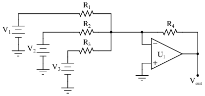
A summing amplifier has multiple inputs and sums them (adds them) all together to create the output. Sometimes, the inputs have equal weightings and sometimes they don’t. Sometimes the output is inverted and sometimes it is non-inverted. See this video to find out about the different configurations
This video describes summing amplifiers and shows the two main configurations. Simulations show that the input voltages do not need to be in phase or even the same frequency, the summer will add them together even if they aren’t sinusoidal.
Summing Amplifier Practice Problems
Question 1. (Click on arrow for answer)
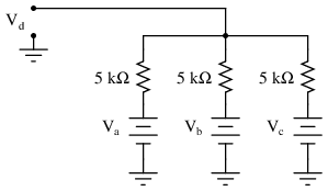
The simple resistor network shown here is known as a passive averager. Describe what the word “passive” means in this context, and write an equation describing the output voltage ([latex]V_d[/latex]) in terms of the input voltages ([latex]V_a[/latex], [latex]V_b[/latex], and [latex]V_c[/latex]):

Hint: there is a network theorem that directly applies to this form of circuit, and it is known as Millman’s Theorem. Research this theorem and use it to generate your equation!
File Num: 01001
Answer
“Passive” means that the circuit contains no amplifying components.[latex]V_d = {{V_a + V_b + V_c} \over 3}[/latex]Notes
Students need to realize that even passive circuits are able to model (some) mathematical functions! Ask your students if they can think of any network analysis methods to easily calculate the output voltage ([latex]V_d[/latex]) of this circuit, given the input voltages. There is one theorem in particular that works very well for this particular circuit.
Question 2. (Click on arrow for answer)
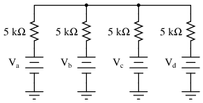
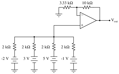
Add an op-amp circuit to the output of this passive averager network to produce a summer circuit: an operational circuit generating an output voltage equal to the sum of the four input voltages. Then, write an equation describing the whole circuit’s function.
\vskip 30pt
File Num: 01002
Answer
 [latex]V_{sum} = V_a + V_b + V_c + V_d[/latex]
Notes
The equation for this circuit is simple enough as to require no explanation. How your students derived this equation, from the base equation of a passive averager network, on the other hand, is worth discussion. Discuss with them the necessary gain of the op-amp circuit, and how this gain figure converts an averaging function into a summing function.
Question 3. (Click on arrow for answer)
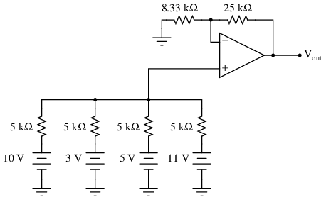
Determine all current magnitudes and directions, as well as voltage drops, in this circuit:

File Num: 02515
Answer

Follow-up question: what would be required to get this circuit to output the exact sum of the four input voltages?
Notes
This question not only provides practice analyzing the behavior of a summer circuit, but also analyzing the behavior of a passive averager circuit. If your students need some refreshing on how to analyze the passive averager, you might want to review Millman’s Theorem with them.
Question 4. (Click on arrow for answer)
Determine all current magnitudes and directions, as well as voltage drops, in this circuit:

File Num: 02523
Answer

Follow-up question: what would be required to get this circuit to output the exact sum of the four input voltages?
Notes
This question not only provides practice analyzing the behavior of a summer circuit, but also analyzing the behavior of a passive averager circuit. If your students need some refreshing on how to analyze the passive averager, you might want to review Millman’s Theorem with them.
Question 5. (Click on arrow for answer)
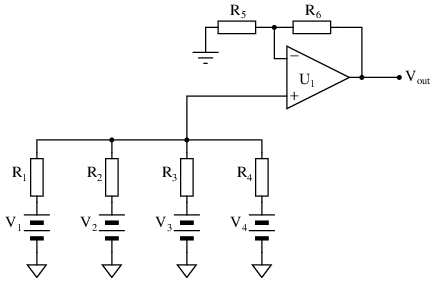
Predict how the operation of this summer circuit will be affected as a result of the following faults. Consider each fault independently (i.e. one at a time, no multiple faults):

- Resistor [latex]R_1[/latex] fails open:
- Solder bridge (short) across resistor [latex]R_3[/latex]:
- Resistor [latex]R_4[/latex] fails open:
- Resistor [latex]R_5[/latex] fails open:
- Solder bridge (short) across resistor [latex]R_5[/latex]:
- Resistor [latex]R_6[/latex] fails open:
For each of these conditions, explain why the resulting effects will occur.
File Num: 03780
Answer
- Resistor [latex]R_1[/latex] fails open: [latex]V_{out[/latex] becomes equal to [latex]{4 \over 3}[/latex] the sum of voltages [latex]V_2[/latex], [latex]V_3[/latex], and [latex]V_4[/latex].}
- Solder bridge (short) across resistor [latex]R_3[/latex]: [latex]V_{out[/latex] becomes equal to 4 times [latex]V_3[/latex].}
- Resistor [latex]R_4[/latex] fails open: [latex]V_{out[/latex] becomes equal to [latex]{4 \over 3}[/latex] the sum of voltages [latex]V_1[/latex], [latex]V_2[/latex], and [latex]V_3[/latex].}
- Resistor [latex]R_5[/latex] fails open:>Circuit operates as an averager, not a summer.
- Solder bridge (short) across resistor [latex]R_5[/latex]: [latex]V_{out[/latex] saturates in a positive direction.}
- Resistor [latex]R_6[/latex] fails open: [latex]V_{out[/latex] saturates in a positive direction.}
Notes
The purpose of this question is to approach the domain of circuit troubleshooting from a perspective of knowing what the fault is, rather than only knowing what the symptoms are. Although this is not necessarily a realistic perspective, it helps students build the foundational knowledge necessary to diagnose a faulted circuit from empirical data. Questions such as this should be followed (eventually) by other questions asking students to identify likely faults based on measurements.
Question 6. (Click on arrow for answer)
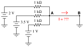
Determine the amount of current from point A to point B in this circuit:

File Num: 02516
Answer
[latex]I[/latex] = 6.5 mANotes
This question, while being an application of Kirchhoff’s Current Law, is also a prelude to an inverting summer circuit, where an opamp takes that 6.5 mA (total) current and converts it into an output voltage.
Question 7. (Click on arrow for answer)
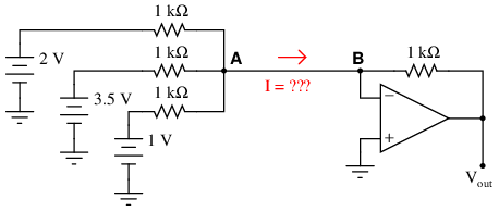
Determine the amount of current from point A to point B in this circuit, and also the output voltage of the operational amplifier:

File Num: 02517
Answer
[latex]I[/latex] = 6.5 mA [latex]V_{out}[/latex] = -6.5 VNotes
This question is best preceded by \#02516, which asks for students to solve for the current between A and B with no opamp in the circuit (simply grounded at point B). When students realize that point B is now a virtual ground instead of a real ground, they see that the same conclusion derived by Kirchhoff’s Current Law in the passive circuit is still valid in this active circuit, and that the result is an output voltage corresponding to that current.
Question 8. (Click on arrow for answer)
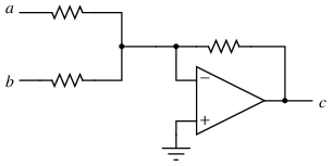
Write a mathematical equation for this op-amp circuit, assuming all resistor values are equal:

What is this circuit typically called?
File Num: 01003
Answer
[latex]c = -(a + b)[/latex]This type of circuit is typically called an inverting summer.
Follow-up question: explain why the addition of another resistor in this circuit is recommended for optimum accuracy, as shown in the following schematic.

Challenge question: write an equation describing the proper value of this extra resistor.
Notes
Ask your students about the proper resistor values for an inverting summer circuit. The choices of resistor values are definitely not the same for inverting summer and noninverting summer circuits alike! Discuss why the values are what they are in an inverting summer circuit (using Ohm’s Law to analyze the circuit’s function), emphasizing comprehension over rote memorization.
Question 9. (Click on arrow for answer)
Predict how the operation of this summer circuit will be affected as a result of the following faults. Consider each fault independently (i.e. one at a time, no multiple faults):

- Resistor [latex]R_1[/latex] fails open:
- Resistor [latex]R_2[/latex] fails open:
- Solder bridge (short) across resistor [latex]R_3[/latex]:
- Resistor [latex]R_4[/latex] fails open:
- Solder bridge (short) across resistor [latex]R_4[/latex]:
For each of these conditions, explain why the resulting effects will occur.
File Num: 03781
Answer
- Resistor [latex]R_1[/latex] fails open: [latex]V_{out[/latex] becomes (inverted) sum of [latex]V_2[/latex] and [latex]V_3[/latex] only.}
- Resistor [latex]R_2[/latex] fails open: [latex]V_{out[/latex] becomes (inverted) sum of [latex]V_1[/latex] and [latex]V_3[/latex] only.}
- Solder bridge (short) across resistor [latex]R_3[/latex]: [latex]V_{out[/latex] saturates in a negative direction.}
- Resistor [latex]R_4[/latex] fails open: [latex]V_{out[/latex] saturates in a negative direction.}
- Solder bridge (short) across resistor [latex]R_4[/latex]: [latex]V_{out[/latex] goes to 0 volts.}
Notes
The purpose of this question is to approach the domain of circuit troubleshooting from a perspective of knowing what the fault is, rather than only knowing what the symptoms are. Although this is not necessarily a realistic perspective, it helps students build the foundational knowledge necessary to diagnose a faulted circuit from empirical data. Questions such as this should be followed (eventually) by other questions asking students to identify likely faults based on measurements.
Question 10. (Click on arrow for answer)
Identify some of the distinguishing characteristics of inverting and noninverting summer circuits. How may you identify which is which, and how may you determine the proper resistor values to make each one work as it should?
File Num: 02520
Answer
I won’t directly answer the questions here, but I will give some hints. A noninverting summer circuit is composed of a passive voltage averager circuit coupled to a noninverting voltage amplifier with a voltage gain equal to the number of inputs on the averager. An inverting summer circuit is composed of a passive current summer node coupled to a current-to-voltage converter.
Notes
This question is designed to spur discussion amongst your students, exchanging ideas about each circuit’s defining characteristics. Having students explore each circuit type on their own, reaching their own conclusions about how to differentiate the two, is a far more effective way of making them understand the differences than simply telling them outright.
Difference Amplifier Circuit
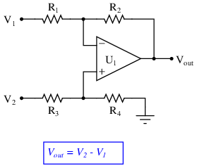
A difference amplifier outputs a voltage that is the difference between two input voltages. The inputs might be equally weighted or they might not be. It depends on the values of the resistors around the op amp. Watch this video to learn more:
This video derives the equation for a difference amplifier given arbitrary values for the resistor around it. As you will see if the resistors are all the same or if R1/R3 are equal and R2/R4 are equal, you get a much easier to analyze circuit.
Difference Amplifier Practice Problems
Question 1. (Click on arrow for answer)
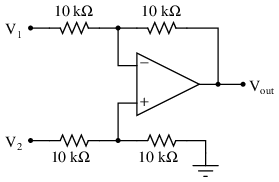
Complete the table of values for this opamp circuit, calculating the output voltage for each combination of input voltages shown:

V1 V2 Vout 0V 0V +1V 0V 0V +1V +2V +1.5V +3.4V +1.2V -2V +4V +5V +5V -3V -3V
What pattern do you notice in the data? What mathematical relationship is there between the two input voltages and the output voltage?
File Num: 02518
Answer
| V1 | V2 | Vout |
|---|---|---|
| 0V | 0V | 0V |
| +1V | 0V | -1V |
| 0V | +1V | +1V |
| +2V | +1.5V | -0.5V |
| +3.4V | +1.2V | -2.2V |
| -2V | +4V | +6V |
| +5V | +5V | 0V |
| -3V | -3V | 0V |
Notes
Though it may be tedious to calculate the output voltage for each set of input voltages, working through all the voltage drops and currents in the opamp circuit one at a time, it shows students how they may be able to discern the function of an opamp circuit merely by applying basic laws of electricity (Ohm’s Law, KVL, and KCL) and the “golden assumptions” of negative feedback opamp circuits (no input currents, zero differential input voltage).
Question 2. (Click on arrow for answer)
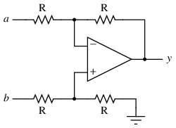
This opamp circuit is known as a difference amplifier, sometimes called a subtractor. Assuming that all resistor values are equal in the circuit, write an equation expressing the output ([latex]y[/latex]) as a function of the two input voltages ([latex]a[/latex] and [latex]b[/latex]):

File Num: 01010
Answer
[latex]y = b – a[/latex]Notes
Work through some example conditions of input voltages and resistor values to calculate the output voltage using Ohm’s Law and the general principle of negative feedback in an opamp circuit (namely, an assumption of zero voltage differential at the opamp inputs). The goal here is to have students comprehend why this circuit subtracts one voltage from another, rather than just encourage rote memorization.
Question 3. (Click on arrow for answer)
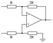
How does the operation of this difference amplifier circuit compare with the resistor values given ([latex]2R[/latex] = twice the resistance of [latex]R[/latex]), versus its operation with all resistor values equal?

Describe what approach or technique you used to derive your answer, and also explain how your conclusion for this circuit might be generalized for all difference amplifier circuits.
File Num: 02525
Answer
It is very important that you develop the skill of “exploring” a circuit configuration to see what it will do, rather than having to be told what it does (either by your instructor or by a book). All you need to have is a solid knowledge of basic electrical principles (Ohm’s Law, Kirchhoff’s Voltage and Current Laws) and know how opamps behave when configured for negative feedback.
As for a generalized conclusion:

Notes
It is easy for you (the instructor) to show how and why this circuit acts as it does. The point of this question, however, is to get students to take the initiative to explore the circuit on their own. It is simple enough for any student to set up some hypothetical test conditions (a thought experiment) to analyze what this circuit will do, that the only thing holding them back from doing so is attitude, not aptitude.
This is something I have noticed over years of teaching: so many students who are more than capable of doing the math and applying well-understood electrical rules refuse to do so on their own, because years of educational tradition has indoctrinated them to wait for the instructor’s lead rather than explore a concept on their own.
Question 4. (Click on arrow for answer)
Predict how the operation of this difference amplifier circuit will be affected as a result of the following faults. Consider each fault independently (i.e. one at a time, no multiple faults):

- Resistor [latex]R_1[/latex] fails open:
- Resistor [latex]R_2[/latex] fails open:
- Solder bridge (short) across resistor [latex]R_3[/latex]:
- Resistor [latex]R_4[/latex] fails open:
- Solder bridge (short) across resistor [latex]R_4[/latex]:
For each of these conditions, explain why the resulting effects will occur.
File Num: 03782
Answer
- Resistor [latex]R_1[/latex] fails open: [latex]V_{out}[/latex] becomes equal to [latex]{1 \over 2}[/latex] [latex]V_2[/latex].}
- Resistor [latex]R_2[/latex] fails open: [latex]V_{out}[/latex] saturates.}
- Solder bridge (short) across resistor [latex]R_3[/latex]: [latex]V_{out}[/latex] becomes equal to [latex]2 V_2 – V_1[/latex] instead of [latex]V_2 – V_1[/latex].}
- Resistor [latex]R_4[/latex] fails open: [latex]V_{out}[/latex] becomes equal to [latex]2 V_2 – V_1[/latex] instead of [latex]V_2 – V_1[/latex].}
- Solder bridge (short) across resistor [latex]R_4[/latex]: [latex]V_{out}[/latex] becomes equal to [latex]-V_1[/latex].}
Notes
The purpose of this question is to approach the domain of circuit troubleshooting from a perspective of knowing what the fault is, rather than only knowing what the symptoms are. Although this is not necessarily a realistic perspective, it helps students build the foundational knowledge necessary to diagnose a faulted circuit from empirical data. Questions such as this should be followed (eventually) by other questions asking students to identify likely faults based on measurements.
Integrator Op Amp Circuit
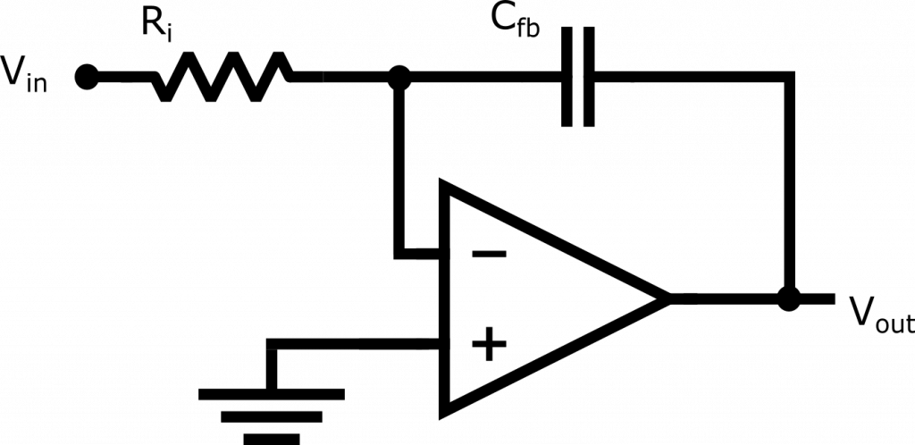
The integrator circuit does exactly what you would think that it does…it takes the input voltage and integrates it to give the output voltage. Yes, circuits can do calculus. To find out how, see the video below
The integrator op amp circuit is an inverting op amp circuit with a resistor at the input and a capacitor for the feedback. This video goes through the analysis to see why it is called an integrator. The video also includes some simulations that show the integrator working and also not working
Differentiator Op Amp Circuit

Once again, the name of the circuit is the thing that it does. So this circuit differentiates, or takes the derivative of the input voltage to create the output voltage. Well, it doesn’t actually sit there and do the calculation, but the output voltage is proportional to the derivative of the input voltage and in this video, I show you why.
The differentiator op amp circuit does output the derivative of the input, but as you will see in this video, it is a little sensitive and unstable.
Contributors
Contributors to this chapter are listed in chronological order of their contributions, from most recent to first.
David Williams (2022): First edits including videos
Practice Problem Copyright
All practice problems with a file num less than 4100 are Copyright 2003, Tony R. Kuphaldt, released under the Creative Commons Attribution License (v 1.0). All other files are Copyright 2022, David Williams, released under the Creative Commons Attribution License (V 4.0) This means you may do almost anything with this work, so long as you give proper credit.
To view a copy of the license, visit https://creativecommons.org/licenses/by/1.0/, or https://creativecommons.org/licenses/by/4.0/, or send a letter to Creative Commons, 559 Nathan Abbott Way, Stanford, California 94305, USA. The terms and conditions of this license allow for free copying, distribution, and/or modification of all licensed works by the general public.


 $$\vbox{\offinterlineskip
\halign{\strut
\vrule \quad\hfil # \ \hfil &
\vrule \quad\hfil # \ \hfil \vrule \cr
\noalign{\hrule}[latex]V_{in}[/latex] & [latex]V_{out}[/latex] \cr\noalign{\hrule}
